
A Comprehensive Guide to Audio Power Amplifier Design
The audio power amplifier is the heart of any high-fidelity sound system. It performs the critical task of taking a low-power audio signal from a source like a DAC or preamplifier and boosting it to a level sufficient to drive loudspeakers [2]. Designing a great amplifier is a multifaceted discipline, touching on everything from fundamental device physics to advanced feedback theory, thermal management, and PCB layout [6].
This article provides a comprehensive overview of audio power amplifier design, covering the fundamental principles, common architectures, key design considerations, and modern trends. Whether you are an electronics student, a seasoned professional, or an audio hobbyist, this guide will help you understand the science and art behind creating powerful, clear sound.
Understanding Amplifier Classes
Amplifier "class" refers to the design of the output stage and how its active devices (transistors or vacuum tubes) are biased. This choice fundamentally dictates the trade-off between **efficiency** and **linearity** (sound fidelity). The most common classes in audio are A, B, AB, and D [14].
Class A
In a **Class A** amplifier, the output transistors are always conducting, regardless of the audio signal. This means they conduct through the full 360 degrees of the signal waveform. This "always-on" state eliminates the distortion that occurs when transistors switch on and off, resulting in the purest sound and highest linearity. However, this comes at a steep price: extremely low efficiency (typically 20-30%) and massive heat generation, as the amplifier dissipates maximum power even at idle [48][49].

Class B
A **Class B** amplifier uses two transistors in a "push-pull" arrangement, where one handles the positive half of the waveform and the other handles the negative half. Each transistor is active for only 180 degrees of the signal. This dramatically improves efficiency (up to ~78.5%) but introduces **crossover distortion**—a nonlinearity that occurs at the zero-crossing point where one transistor turns off and the other turns on [47].
Class AB
As a hybrid of the two, **Class AB** is the most common design for high-fidelity amplifiers. It is essentially a Class B design but with a small amount of **quiescent (idle) current** flowing through both output transistors at all times. This small bias is enough to keep the transistors "on" through the crossover region, significantly reducing crossover distortion while maintaining much of Class B's efficiency (typically 50-70%) [13][47]. It represents a well-balanced compromise between performance and efficiency.

Class D
Often mistakenly called "digital amplifiers," **Class D** amplifiers are highly efficient switching amplifiers. They work by converting the analog audio signal into a high-frequency **Pulse Width Modulated (PWM)** signal. This PWM signal rapidly switches the output transistors fully on or off—states where they dissipate very little power. A passive low-pass filter at the output then reconstructs the amplified analog audio signal and removes the high-frequency switching noise [47]. Class D amplifiers can achieve efficiencies exceeding 90%, making them ideal for compact, high-power applications like car audio, portable speakers, and professional sound systems [48][21].

Class G & H
Class G and H are advanced variations that improve efficiency over Class AB by using multiple or tracking power supply rails. A **Class H** amplifier, for instance, switches between different fixed supply voltage rails depending on the signal level, while a **Class G** amplifier modulates the supply voltage to track the signal envelope. This reduces power dissipation by providing just enough voltage for the required output swing, making them suitable for high-performance systems where power management is critical [48][56].
Class T
Class T amplifiers are a special type of audio amplifier that combine elements of Class D switching amplifiers with digital signal processing (DSP) to achieve high efficiency and excellent sound quality. Unlike traditional Class D amplifiers that rely solely on fixed-frequency pulse-width modulation (PWM), Class T uses advanced modulation schemes and feedback control to optimize performance in real time. One well-known example of a Class T amplifier is the Tripath TA2020 chip, which was highly regarded for delivering transparent and dynamic sound in a tiny power module.

| Amplifier Class | Efficiency | Sound Quality | Heat Generation | Ideal Use |
|---|---|---|---|---|
| Class A | Low | Best (Purest Sound) | High | Audiophile home systems |
| Class B | High | Good (Slight Distortion) | Moderate | General use (less common now) |
| Class AB | Moderate | Very Good | Moderate | Home audio, car audio, balanced choice |
| Class D | Very High | Good to Excellent | Low | Portable systems, subwoofers, pro audio |
| Class H/G | High | Good | Low | High-performance, power-sensitive systems |
Core Architecture of a Solid-State Power Amplifier
Most modern solid-state power amplifiers, particularly Class AB designs, follow a well-established three-stage architecture. This structure has evolved to effectively address performance deficiencies and optimize linearity [4].
1. Input Stage (IPS)
The input stage is typically a **differential amplifier** (often called a "long-tailed pair"). Its primary functions are:
- To receive the incoming audio signal at one input and the negative feedback signal from the amplifier's output at the other.
- To subtract these two signals, producing an error signal that the rest of the amplifier works to minimize.
- To provide some initial voltage gain and set the overall DC operating conditions.
The choice of transistors for the input stage—**Bipolar Junction Transistors (BJTs)** or **Junction Field-Effect Transistors (JFETs)**—has significant implications. BJTs offer better matching for low DC offset, while JFETs provide a very high input impedance and eliminate input bias current issues, which can simplify DC servo design [4].
2. Voltage Amplification Stage (VAS)
The VAS is responsible for providing the majority of the amplifier's **voltage gain**. It is typically a common-emitter stage that takes the error signal from the input stage and amplifies it to a level high enough to drive the output stage. The VAS has a high-impedance output, making it sensitive to loading. Therefore, it must be effectively buffered by the output stage [4].
3. Output Stage (OPS)
The output stage is a **current amplifier**. It has a voltage gain of slightly less than unity but provides the high current necessary to drive low-impedance loudspeaker loads. It acts as a buffer, isolating the high-impedance VAS from the speaker.
Common configurations include the **Darlington pair** (a "Double") or, for better performance, the **Triple Emitter Follower** (also known as a "Triple" or Locanthi T circuit). The Triple provides much higher current gain, which better isolates the VAS from the load, especially at high output currents and with low-impedance speakers. This increased buffering significantly reduces distortion caused by effects like beta droop in the output transistors [4].
Key Design Principles and Calculations
A successful amplifier design relies on careful calculation and consideration of several key parameters.
Gain Calculation
One of the first questions in amplifier design is, "What gain should I use?" The goal is to set the gain just high enough to achieve the desired maximum output power from the maximum input signal level. Setting the gain too high unnecessarily amplifies the noise floor of the source (e.g., a DAC or CODEC), reducing the system's overall **Signal-to-Noise Ratio (SNR)** and dynamic range [18].
The process involves:
- Calculate Required Output Voltage (VO(RMS)): Based on the target output power (PO) and speaker impedance (RL).
VO(RMS) = sqrt(PO * RL) - Determine Input Voltage (VI(RMS)): Convert the peak-to-peak voltage from the source (VI(PP)) to RMS.
VI(RMS) = VI(PP) / (2 * sqrt(2)) - Calculate Required Gain: The required voltage gain (Av) is the ratio of the required output RMS voltage to the available input RMS voltage.
Gain (Av) = VO(RMS) / VI(RMS)
For a typical inverting amplifier configuration, the gain is set by the ratio of the feedback resistor (RF) to the input resistor (RI). You choose standard resistor values to approximate this calculated gain [18].
Power Dissipation and Thermal Management
Thermal management is arguably the most critical aspect of ensuring an amplifier's reliability and long-term performance [25]. Inefficient designs, like Class A and AB, convert a significant portion of input power into heat. This heat must be effectively removed to keep the output transistor junction temperatures within their safe operating limits (typically below 150°C) [63].
Calculating Power Dissipation (Class AB)
The power dissipated in a Class AB output stage (PD) is the difference between the power drawn from the supply (PS) and the power delivered to the load (PL). The dissipation varies with the output signal level, reaching its maximum not at full power, but at a specific output voltage.
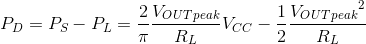
The peak power dissipation occurs when the output voltage swing is VOUTpeak = (2/π) * VCC. The maximum power dissipation can be calculated as:

For example, for an amplifier with ±25V supplies, a 4Ω load, and 50mA bias current, the peak dissipation is approximately 34.2W [64].
Heatsink Selection
Once the maximum power dissipation is known, a suitable **heatsink** can be selected. The heatsink's ability to dissipate heat is defined by its **thermal resistance (θSA)**, measured in °C/W. This value indicates how many degrees Celsius the heatsink's temperature will rise above ambient for every watt of dissipated power.
The total thermal resistance from the transistor's internal junction to the ambient air is the sum of several resistances in series:
- θJC (Junction-to-Case): The thermal resistance from the silicon die to the transistor's package.
- θCS (Case-to-Sink): The resistance of the thermal interface material (e.g., mica washer or silicone pad) between the transistor and the heatsink.
- θSA (Sink-to-Ambient): The thermal resistance of the heatsink itself.
The final junction temperature can be calculated as: Tjunction = Tambient + Pdissipated * (θJC + θCS + θSA) [64]. The goal is to choose a heatsink with a low enough θSA to keep Tjunction well below the component's maximum rating.
Modern Thermal Solutions
To combat thermal instability and distortion caused by temperature fluctuations, modern components like ON Semiconductor's **ThermalTrak™** power transistors have been introduced. These devices integrate a temperature-sensing diode directly on the transistor die. This allows for much faster and more accurate tracking of the power transistor's junction temperature, enabling the bias circuit to adjust almost instantaneously and greatly reducing thermal lag distortion [4].
Advanced Design Topics & Modern Trends
The field of amplifier design is constantly evolving, with new technologies and techniques pushing the boundaries of performance and efficiency.
Class D Amplifiers: Efficiency and Fidelity
While early Class D designs were relegated to low-fidelity applications like subwoofers, modern Class D amplifiers offer performance that rivals or even exceeds traditional Class AB designs. Key innovations include:
- Higher Switching Frequencies: Increasing the PWM switching frequency (e.g., to 2.1 MHz, well above the AM radio band) pushes the switching artifacts and noise much further out of the audio band. This allows for simpler output filters and reduces distortion within the audible range, as there is more loop gain available for error correction [45].
- Advanced Modulation and Feedback: Sophisticated modulation schemes and post-filter feedback loops help to linearize the amplifier's output, correct for power supply variations, and make the performance less dependent on speaker impedance [58].
- Gallium Nitride (GaN) Transistors: The adoption of **GaN** power transistors is a major trend. Compared to traditional silicon MOSFETs, GaN devices offer lower on-resistance, faster switching speeds, and zero reverse recovery charge. This leads to higher efficiency, less heat, smaller form factors, and a significant reduction in distortion, enabling a more precise and detailed sound [32][34].
Vacuum Tube Amplifiers and the Output Transformer
Vacuum tube amplifiers remain cherished by many audiophiles for their characteristic "warm" sound. A key component that distinguishes them from solid-state designs is the **output transformer (OPT)**.
Tubes are high-voltage, low-current devices with a very high output impedance (thousands of ohms). In contrast, loudspeakers are low-impedance devices (typically 4 or 8 ohms). The OPT is an impedance-matching device that steps down the high voltage/impedance from the tubes to the low voltage/impedance required by the speaker, allowing for efficient power transfer [68].
The design of the OPT is critical to the amplifier's performance, influencing its frequency response, distortion, and damping factor. Key design parameters include:
- Primary Inductance (Lp): Determines the low-frequency response. A higher inductance is needed to extend bass response without saturation.
- Turns Ratio (n): Sets the impedance matching between the tubes' plate-to-plate resistance (Raa) and the speaker load (RL).
n = sqrt(Raa / RL). - Leakage Inductance and Winding Capacitance: These parasitic elements determine the high-frequency response. Careful winding techniques, such as **interleaving** (alternating primary and secondary windings), are used to minimize them and extend the bandwidth.


Integrated Circuit (IC) Power Amplifiers
For many applications, integrated circuit (IC) amplifiers offer a compact, reliable, and high-performance solution. Chips like the **TDA7294** and **LM3886** have been staples of the DIY audio community and commercial products for years. These ICs integrate the entire amplifier—input stage, VAS, output stage, and protection circuitry—into a single package [35].


![[73]](https://www.kasuo.com/wp-content/uploads/2025/05/TDA7294-Pinout.jpg)
![[74]](https://www.kasuo.com/wp-content/uploads/2025/05/LM3886.jpg)
The TDA7294, for example, is a DMOS power amplifier capable of delivering up to 100W. It includes features like mute and standby functions, short-circuit protection, and thermal shutdown [36]. A typical mono application circuit is relatively simple, requiring only a handful of external components for gain setting, feedback, and power supply filtering.

For even more power, two ICs can be used in a **Bridge-Tied Load (BTL)** configuration. In this setup, one amplifier drives the speaker's positive terminal and a second, identical amplifier drives the negative terminal with an inverted signal. This doubles the voltage swing across the load, theoretically quadrupling the output power [37].

Practical Implementation: PCB Layout and Protection
A brilliant circuit schematic can be ruined by poor physical implementation. Proper **Printed Circuit Board (PCB) layout** and robust **protection circuits** are essential for a stable, quiet, and reliable amplifier.
PCB Layout Best Practices
Good PCB layout is crucial for minimizing noise, hum, and distortion.
- Grounding: A well-designed ground system is paramount. A **star ground** topology, where all ground connections meet at a single point (usually at the power supply capacitors), is a classic approach to prevent ground loops. Alternatively, carefully implemented ground planes can also be effective, especially in multi-layer boards [27].
- Trace Separation: Keep sensitive, low-level analog input traces physically separated from high-current power supply and output traces. Routing them on different layers with a ground plane in between provides excellent shielding [27].
- Power Supply Decoupling: Place small ceramic capacitors (e.g., 0.1µF) as close as possible to the power pins of ICs and transistors. These provide a local reservoir of charge for high-frequency currents, preventing noise from propagating through the power supply rails. Larger bulk electrolytic capacitors (10µF or more) should be placed nearby for lower-frequency transient demands [27].
- Thermal Layout: Place high-power components like output transistors and heatsinks near the edge of the board to improve airflow. Use **thermal vias** under surface-mount power devices to conduct heat to large copper planes on other layers, effectively turning the PCB itself into part of the heatsink [25].
Protection Circuits
A good protection system serves two purposes: protecting the amplifier from fault conditions and protecting the loudspeakers from amplifier failure [50].
- Overload Protection: This circuitry monitors the output voltage and current to ensure the output transistors remain within their **Safe Operating Area (SOA)**. If a short circuit or excessive load is detected, the circuit limits the drive current to prevent the transistors from being destroyed [4].
- DC Fault Protection: If an amplifier fails, it can output a large DC voltage, which can quickly destroy a loudspeaker's voice coil. A DC protection circuit monitors the output for DC and, if detected, uses a relay to disconnect the speaker [52].
- DC Servo: To eliminate DC offset at the output during normal operation, a **DC servo** is often used. This is an auxiliary feedback loop using an integrator (typically an op-amp) that senses the DC level at the output and injects a small correction current into the input stage to force the output DC to zero. This is a more elegant solution than using a large, sound-degrading DC-blocking capacitor in the signal path [4].
Simulation and Measurement
Before committing a design to hardware, modern engineers rely heavily on circuit simulation to verify and optimize performance.
SPICE Simulation
SPICE (Simulation Program with Integrated Circuit Emphasis)** is an invaluable tool that allows designers to build a virtual prototype of their amplifier. Software like the free and powerful **LTspice** from Analog Devices (formerly Linear Technology) can be used to perform various analyses [4][60]:
- .OP (DC Operating Point): Verifies bias voltages and currents throughout the circuit.
- .AC (AC Analysis): Plots the frequency and phase response to check bandwidth and stability (gain/phase margins).
- .TRAN (Transient Analysis): Simulates the circuit's response to a time-varying signal, allowing for the analysis of waveforms and distortion.
SPICE simulation can save countless hours of lab work by helping to evaluate different circuit topologies, optimize component values, and identify potential issues like instability before a single component is soldered [4].
Key Performance Measurements
Once a prototype is built, its performance must be verified through measurement. Common audio amplifier tests include [30]:
- Total Harmonic Distortion + Noise (THD+N): Measures the unwanted harmonics and noise added by the amplifier. Lower is better.
- Frequency Response: Measures the amplifier's gain across the audio spectrum (typically 20Hz to 20kHz). A flat response is desired.
- Signal-to-Noise Ratio (SNR): The ratio of the maximum signal level to the residual noise floor. Higher is better.
- Damping Factor: The ratio of the speaker's impedance to the amplifier's output impedance. A high damping factor indicates good control over the speaker cone's movement.
Conclusion
Audio power amplifier design is a rich and rewarding field that blends scientific principles with engineering artistry. From the fundamental trade-offs of amplifier classes to the intricate details of feedback, thermal management, and PCB layout, every decision impacts the final sound quality. The journey from a simple three-stage concept to a high-performance, reliable product requires a holistic approach that considers the circuit, its physical implementation, and its interaction with the real world.
As technology marches forward, the trend is toward ever-greater efficiency and integration. The rise of advanced Class D amplifiers, powered by cutting-edge technologies like GaN transistors and sophisticated digital control, is redefining what is possible in terms of performance, size, and power consumption [21]. Yet, the classic principles of analog design remain as relevant as ever, forming the foundation upon which all great amplifiers are built.
References
- [1] John L. Linsley Hood. (2023, December 14). Analog Audio Amplifier Design. Retrieved from https://api.pageplace.de/preview/DT0400.9781000998931_A47027235/preview-9781000998931_A47027235.pdf
- [2] Semantic Scholar. (2024, August 31). Audio Power Amplifier. Retrieved from https://pdfs.semanticscholar.org/a785/232609c8ac15e418875f7dc60a3ce08c9f18.pdf
- [3] Taylor & Francis. Analog Audio Amplifier Design. Retrieved from https://www.taylorfrancis.com/books/mono/10.4324/9781003369462/analog-audio-amplifier-design-john-lam
- [4] Bob Cordell. (2018, September 24). Designing Audio Power Amplifiers. Retrieved from https://pearl-hifi.com/06_Lit_Archive/14_Books_Tech_Papers/Cordell_Bob/Designing_Audio_Pwr_Amps_Cordell.pdf
- [5] UCLA Physics & Astronomy. (2025, December 3). Designing Audio Power Amplifiers From Theory to Practical Implementation. Retrieved from https://aichat.physics.ucla.edu/HomePages/Resources/odppps/Designing-Audio-Power-Amplifiers.pdf
- [6] Cordell Audio. (2025, June 2). Preface to Designing Audio Power Amplifiers. Retrieved from https://www.cordellaudio.com/book/Book2_Preface.pdf
- [7] SpringerLink. (2025, June 26). AI Cyber-Physical Systems and Audio Power Amplifiers. Retrieved from https://link.springer.com/chapter/10.1007/978-3-031-97051-1_29
- [8] MDPI. (2024, November 12). Heatsink Dimensions for Amplifiers. Retrieved from https://www.mdpi.com/2079-9292/14/1/34
- [9] Crown Audio. (2025, November 18). Live Entertainment Audio Systems. Retrieved from https://www.crownaudio.com/zh/case_studies/application/live-entertainment
- [10] ProSoundWeb. (2025, December 22). Real-World Gear: The Latest Power Amplifiers 2025. Retrieved from https://www.prosoundweb.com/real-world-gear-the-latest-power-amplifiers-2025/
- [11] Semiconductor Insight. Global Class-D Audio Power Amplifiers Market. Retrieved from https://semiconductorinsight.com/report/global-class-d-audio-power-amplifiers-market/
- [12] Accio. (2025, September 28). Power Amplifier Professional Trends 2025. Retrieved from https://www.accio.com/business/power-amplifier-professional-trends
- [13] DZSC. (2024, November 14). Class AB Amplifier Principles. Retrieved from https://www.dzsc.com/data/2024-11-14/131257.html
- [14] Wonderful PCB. Class A, B, AB, C, D Amplifier Circuits Comparison. Retrieved from https://www.wonderfulpcb.com/zh-TW/blog/class-a-b-ab-c-d-amplifier-circuits-comparison/
- [15] CMIgo. (2025, December 25). Audio Power Amplifier Design Handbook. Retrieved from https://cmigo.com/index_htm_files/virtual-library/da92Sx/AudioPowerAmplifierDesignHandbook.pdf
- [16] DIY Audio. (2024, July 6). High Fidelity Audio Power Amplifier Design. Retrieved from https://www.diyaudio.com/community/attachments/tp_amplifiers-pdf.45828/
- [17] My New Microphone. (2020, July 3). Complete Guide to Power Amplifier Specifications. Retrieved from https://mynewmicrophone.com/complete-guide-to-power-amplifier-specifications-data/
- [18] Texas Instruments. Calculating Gain for Audio Amplifiers (SLOA105A). Retrieved from https://www.ti.com/lit/an/sloa105a/sloa105a.pdf
- [19] True Geometry. (2024, October 7). Audio Amplifier Calculations. Retrieved from https://blog.truegeometry.com/calculators/Audio_amplifiers_calculation.html
- [20] Analog Devices. (2015, March 6). Amplifier and Filter Design Equations. Retrieved from https://www.analog.com/media/en/selection-guides/Equation_Pullout.pdf
- [21] Accio. (2025, September 10). Latest Class D Amplifier Trends. Retrieved from https://www.accio.com/business/latest-class-d-amplifier-trends
- [22] IEEE Xplore. (2025, September 8). Digital-input class-D audio amplifier with double-sided voltage-boosting. Retrieved from https://ieeexplore.ieee.org/document/11153033
- [23] MDPI. (2024, November 12). Non-circuit-based approach for increasing efficiency of Class AB audio amplifiers. Retrieved from https://www.mdpi.com/2079-9292/14/1/34
- [24] Texas Instruments. (2023, April 1). Thermal Design Considerations for TAS5805M Class-D Audio Amplifier (SLAA880). Retrieved from https://www.ti.com/lit/pdf/slaa880
- [25] ALLPCB. (2025, August 15). Thermal Management in Audio Amplifier PCBs. Retrieved from https://www.allpcb.com/blog/pcb-knowledge/thermal-management-in-audio-amplifier-pcbs-strategies-for-high-power-designs.html
- [26] Infineon Technologies. (2025, January 15). Layout of a Class D Amplifier (AN-1135). Retrieved from https://www.infineon.com/assets/row/public/documents/24/42/an-1135.pdf?fileId=5546d462533600a401535599e83610bf
- [27] JLCPCB. Hi-Fi Amplifier PCB Design. Retrieved from https://jlcpcb.com/blog/hi-fi-amplifier-pcb-design
- [28] DIY Audio. (2025, February 9). Distortion Measurement Techniques. Retrieved from https://www.diyaudio.com/community/attachments/bridge-null-distortion-measurement_r1a-pdf.1395474/
- [29] Texas Instruments. (2023, April 1). Measuring Audio Power Amplifier Performance (SLOA068A). Retrieved from https://www.ti.com/lit/an/sloa068a/sloa068a.pdf
- [30] Audio Precision. What are the most common measurements for amplifier testing?. Retrieved from https://www.ap.com/applications/amplifier-testing/what-are-the-most-common-measurements-for-amplifier-testing
- [31] ScienceDirect. (2025, January 1). Gallium nitride (GaN) device for power amplifier applications. Retrieved from https://www.sciencedirect.com/science/article/pii/S2667325823003023
- [32] All About Circuits. (2025, March 5). The GaN-Powered Future of Class-D Audio Amplifiers. Retrieved from https://www.allaboutcircuits.com/industry-articles/breaking-barriers-in-sound-the-gan-powered-future-of-class-d-audio-amplifiers/
- [33] ELEPCB. (2025, June 24). Amplifier PCB Design. Retrieved from https://www.elepcb.com/blog/amplifier-pcb-design/
- [34] Infineon Technologies. (2025). Infineon’s CoolGaN™ transistors improve sound quality and efficiency of SounDigital’s Class D amplifier. Retrieved from https://www.infineon.com/market-news/2025/infpss202502-061
- [35] EEFocus. (2023, February 9). TDA7294 and LM3886 Comparison. Retrieved from https://www.eefocus.com/e/1414039.html
- [36] Kasuo. TDA7294 Datasheet vs LM3886. Retrieved from https://www.kasuo.com/zh/product/tda7294-datasheet-vs-lm3886/
- [37] Botland. (2024, October 5). TDA7294 Audio Amplifier Sample Circuits. Retrieved from https://botland.store/blog/tda7294-audio-amplifier-sample-circuits/
- [38] Douglas Self. Audio Power Amplifier Design Handbook. Retrieved from https://www.sciencedirect.com/book/monograph/9780240521626/audio-power-amplifier-design-handbook
- [39] Douglas Self. (2015, May 21). Audio Power Amp Design Handbook 4th Edn. Retrieved from https://nick.desmith.net/Data/Books%20and%20Manuals/Self%20-%20Audio%20Power%20Amp%20Design%20Handbook%204th%20Edn.pdf
- [40] KKPCBA. (2025, September 17). Case Study: High-Fidelity Audio Amplifier PCB. Retrieved from https://www.kkpcba.com/kkpcb-case-study-high-fidelity-audio-amplifier-pcb-for-premium-audio-applications/
- [41] JBL Professional. Case Studies. Retrieved from https://jblpro.com/en/case_studies
- [42] Harman Professional. (2023, March 29). JBL Pro AE Application Engineered Loudspeaker Installations. Retrieved from https://pro.harman.com/insights/jbl-pro/around-the-world-exploring-8-best-in-class-jbl-pro-ae-application-engineered-loudspeaker-installations/
- [43] Zhihu. (2023, June 29). Specialized Loudspeaker Characteristics. Retrieved from https://zhuanlan.zhihu.com/p/640500745
- [44] Texas Instruments. (2023, April 1). Characterizing Audio Amplifier Thermal Performance (SLOA104). Retrieved from https://www.ti.com/lit/an/sloa104/sloa104.pdf
- [45] Texas Instruments. (2025, June 12). Designing a Premium Automotive Audio System. Retrieved from https://www.ti.com/content/dam/videos/external-videos/en-us/3/3816841626001/5769850319001.mp4/subassets/designing_a_premium_audio_system.pdf
- [46] SpringerLink. (2025, May 21). Challenges in Electronic Technology. Retrieved from https://link.springer.com/article/10.1007/s10470-025-02422-z
- [47] Pult.ae. (2025, March 13). Understanding Amplifier Classes: A, B, AB, and D. Retrieved from https://pult.ae/media/articles/understanding-amplifier-classes-a-b-ab-and-d
- [48] Nottingham HiFi. (2025, May 1). Which Class Audio Amplifier?. Retrieved from https://nottinghamhifi.co.uk/blogs/blog/which-class-audio-amplifier
- [49] Peter Tyson. Hi-Fi Amplifier Classes Explained. Retrieved from https://petertyson.co.uk/blog/hi-fi-amplifier-classes-explained
- [50] Linear Audio. (2023, January 23). Amplifier Protection Systems. Retrieved from https://linearaudio.net/sites/linearaudio.net/files/UK-3%202008050501.pdf
- [51] Homemade Circuits. (2025, April 6). Amplifier Short/Overload Protection. Retrieved from https://www.homemade-circuits.com/make-this-amplifier-shortoverload/
- [52] Sound-au.com. (2025, July 22). Amplifier Powered DC Protection Circuit. Retrieved from https://sound-au.com/project208.htm
- [53] Georgia Tech. (2025, February 21). Practical Approach to Amplifier Output Stage Design. Retrieved from https://www.diyaudio.com/community/attachments/davideatherprac1-pdf.656150/
- [54] Sound-au.com. (2006, December 27). Amplifier Design Techniques. Retrieved from https://sound-au.com/amp_design.htm
- [55] ETHW. (2023, December 5). Audio Transformer Design for Tube Amplifiers. Retrieved from https://ethw.org/w/images/c/cc/Audio_transformer_design_tube_amplifier_pichkalyov_final_paper.pdf
- [56] SpringerLink. (2025, June 26). Energy efficiency in audio amplifiers for mobile devices. Retrieved from https://link.springer.com/chapter/10.1007/978-3-031-97051-1_29
- [57] ResearchGate. (2025, July 8). High-Performance Audio Power Amplifier with a Push-Pull Voltage Amplification Stage. Retrieved from https://www.researchgate.net/publication/394359717_High-Performance_Audio_Power_Amplifier_with_a_Push-Pull_Voltage_Amplification_Stage_and_Active_Loads_in_the_Input_Differential_Pair
- [58] Academia.edu. Design Methodologies for Switch Mode (Class D) Audio Power Amplifiers. Retrieved from https://www.academia.edu/Documents/in/Audio_Amplifiers
- [59] LinkedIn. Gan-on-sic Power Amplifier Market Trends. Retrieved from https://www.linkedin.com/pulse/gan-on-sic-power-amplifier-market-trends-strategic-8omtf
- [60] Analog Devices. (2025, December 26). LTspice Simulator. Retrieved from https://www.analog.com/cn/resources/design-tools-and-calculators/ltspice-simulator.html
- [61] YouSpice. (2015, April 16). Full Course Designing Three Stages Audio Power Amplifiers. Retrieved from https://youspice.com/spiceprojects/spice-simulation-projects/audio-circuits-spice-simulation-projects/power-amplifiers-spice-simulation-projects/discrete-component-power-amplifiers-spice-simulation-projects/full-course-designing-three-stages-audio-power-amplifiers/
- [62] Texas Instruments. Design & simulation tools. Retrieved from https://www.ti.com.cn/zh-cn/design-development/design-simulation-tools.html/
- [63] Pearl-hifi.com. (2018, September 24). How to Spec Heatsinks. Retrieved from https://pearl-hifi.com/06_Lit_Archive/15_Mfrs_Publications/Bybee_Noise_Reduction/How_to_Spec_Heatsinks.pdf
- [64] Neurochrome. Thermal Design. Retrieved from https://neurochrome.com/pages/thermal-design
- [65] Linear Audio. TPC and TMC Feedback Compensation in Power Amplifiers. Retrieved from https://linearaudio.net/tpc-and-tmc-feedback-compensation-power-amplifiers
- [66] Leach Legacy. (2006, October 9). Feedforward Frequency Compensation. Retrieved from https://leachlegacy.ece.gatech.edu/papers/Feedforward.pdf
- [67] Taylor & Francis. Feedback Compensation. Retrieved from https://www.taylorfrancis.com/chapters/mono/10.4324/9781003327943-12/feedback-compensation-robert-buono
- [68] Home Theater HiFi. (2025, September 25). Why Tube Power Amplifiers Require Output Transformers. Retrieved from https://hometheaterhifi.com/technical/primers/why-tube-power-amplifiers-require-output-transformers-and-why-their-design-is-critical/
- [69] Discivio. (2025, November 21). Understanding Amplifier Transformers. Retrieved from https://discivio.com/articles/understanding-amplifier-transformers/
- [70] IEEE Xplore. (2024, November 8). Design and Optimization of a Class AB Audio Amplifier. Retrieved from https://ieeexplore.ieee.org/document/10797394
- [71] ResearchGate. (2025, April 14). Enhancing Audio Performance: Noise Reduction and Efficiency in Class AB Amplifier Design. Retrieved from https://www.researchgate.net/profile/Bonciog-Dumitru-Daniel-2/publication/387290131_Enhancing_Audio_Performance_Noise_Reduction_and_Efficiency_in_Class_AB_Amplifier_Design/links/678e58161ec9f9589f51b900/Enhancing-Audio-Performance-Noise-Reduction-and-Efficiency-in-Class-AB-Amplifier-Design.pdf
- [72] Infineon Technologies. (2025, April 29). Optimize Signal Gain in Class D Amplifiers to Achieve More Than 110 dB SNR. Retrieved from https://www.infineon.com/assets/row/public/documents/24/42/infineon-dg221820-optimize-signal-gain-in-class-d-amplifiers-to-achieve-more-than-110-db-snr-applicationnotes-en.pdf?fileId=8ac78c8c9625080601968046450a037c
- [73] Kasuo. TDA7294 Pinout. Retrieved from https://www.kasuo.com/wp-content/uploads/2025/05/TDA7294-Pinout.jpg
- [74] Kasuo. LM3886 Image. Retrieved from https://www.kasuo.com/wp-content/uploads/2025/05/LM3886.jpg