Transistor Matching for Audio Amplifiers: Why It Matters and How to Do It Right
PUBLISHED BY IWISTAO · DIY Audio / Electronics
A practical guide to matching bipolar transistors in audio circuits — from differential input pairs to parallel output stages, with real-world examples from popular amplifier designs.
Introduction
Walk into any serious DIY audio forum and you will see builders swapping stories about transistor matching. Some treat it as a rite of passage; others dismiss it as audiophile voodoo. The reality lies somewhere in between. Matching transistors does not magically transform an average amplifier into a world-class design, nor does it improve frequency response or transient behavior. What it does do — when done correctly — is improve DC stability, reduce distortion in specific circuit topologies, ensure reliable current sharing in parallel output stages, and minimize offset voltage in differential input stages.

This article explains what transistor matching actually achieves, which parameters matter, and how to match transistors in practice. We use concrete examples from real audio circuits — differential input pairs built with 2SC2240/2SA970, VAS stages using 2N5551/2N5401, and output stages with MJL3281/MJL1302 power devices.
Why Match Transistors in Audio Circuits?
1. Differential Input Stages
The differential pair (also called a long-tailed pair) is the most common input stage in solid-state audio amplifiers. It consists of two identical transistors sharing a common emitter (or source) current. The difference between the two base voltages is amplified and passed to the next stage.
When the two transistors are not matched, the differential pair generates a DC offset voltage at its output. This offset propagates through the amplifier chain and appears as unwanted DC at the speaker terminals. More subtly, unmatched pairs produce higher even-order harmonic distortion because the transfer curves of the two devices differ [1].
In a typical power amplifier with a differential BJT input pair, matching the transistors to within 2 mV of Vbe and 10% of hFE reduces DC offset at the output from potentially hundreds of millivolts to well under 50 mV — without relying on a DC servo [2].
The most widely used transistor pair for audio differential input stages is the 2SC2240 (NPN) and 2SA970 (PNP) from Toshiba. These are low-noise audio transistors, but their noise figure depends strongly on source resistance and collector current. Typical datasheet NF values for the 2SC2240 are around 2–4 dB under specified test conditions (e.g., RG = 100 Ω, VCE = 6 V, IC = 100 µA, f = 1 kHz), while the 2SA970 is typically around 3 dB — not a universal 1 dB figure. Their transition frequency (fT) of 100 MHz ensures excellent linearity throughout the audio band.

Figure 1: A BJT differential pair (long-tailed pair), the most common input stage in audio power amplifiers. Matching Q1 and Q2 for Vbe and hFE minimizes DC offset at the output.
2. Complementary Pairs and VAS Stages
The voltage amplifier stage (VAS) of most power amplifiers uses a complementary pair of NPN and PNP transistors. Common choices include the 2N5551 (NPN) and 2N5401 (PNP) — high-voltage devices rated at Vceo = 160 V and Ic = 600 mA, with fT around 100 MHz. These are workhorse transistors found in countless amplifier designs.
In a push-pull VAS, mismatched NPN and PNP gain creates asymmetry in the drive signal delivered to the output stage. This asymmetry shows up as elevated second-harmonic distortion. Matching hFE between the complementary devices — at the actual operating current of the VAS, typically 5–20 mA — brings the positive and negative half-cycles into balance.
Some low-feedback amplifier designs absolutely require that NPN and PNP transistors be matched, because there is insufficient feedback to linearize the circuit unless the devices track each other closely [3].
3. Parallel Output Stages
High-power amplifiers routinely use multiple output transistors in parallel to handle the required current. If these transistors are not matched, the device with the highest gain (or lowest Vbe) hogs the current, runs hotter, and becomes even more conductive — a runaway condition that can destroy the output stage.
For parallel output transistors, both Vbe and hFE must be matched. A good target is ±10 mV for Vbe and within 10% for hFE at the quiescent current and at a current near the expected peak [3]. The popular MJL3281A (NPN) / MJL1302A (PNP) power pair from ON Semiconductor — rated at 260 V / 15 A / 200 W with fT = 30 MHz — is a common choice for high-end output stages and benefit significantly from matching.

Figure 2: Two matched MJL3281A output transistors in parallel. Matching Vbe and gain reduces the risk of current hogging, while emitter resistors, proper bias compensation, and common heatsinking provide the main protection against thermal runaway. The 0.1Ω emitter resistors provide additional current-sharing assistance.
Key Parameters to Match
hFE (DC Current Gain)
hFE is an important matching parameter, but it is not always the most important one. For differential input pairs, Vbe or collector current at the same bias condition often matters more for DC offset. For parallel output devices, Vbe, gain, emitter resistors, and thermal coupling all determine current sharing. hFE = Ic / Ib varies with collector current, temperature, and even between devices from the same production batch. Most transistor datasheets specify hFE at one or two current points, but real-world audio circuits operate across a wide range. A matching approach that tests only at a single current — say, 1 mA — overlooks gain differences that appear at 10 mA or 100 µA.
Many Japanese transistors, including the 2SC2240 and 2SA970, are sold in hFE classification ranks marked by a suffix letter on the package. The standard Toshiba ranks for these devices are:
| hFE Rank | Gain Range (Vce = 6V, Ic = 1mA) | Typical Use |
|---|---|---|
| O | 100 – 200 | General purpose |
| Y | 120 – 240 | Standard audio |
| GR | 200 – 400 | Low-noise preamp / phono |
| BL | 350 – 700 | High-gain, low-noise input |
Buying transistors from the same hFE rank is a good start, but even within the same rank, individual devices can vary by a factor of two. For critical differential pairs, further hand-matching is essential.
Vbe (Base-Emitter Voltage)
For BJTs operated in parallel, Vbe matching is as important as gain matching. Vbe has a temperature coefficient of approximately −2 mV/°C, so temperature differences between devices can easily overwhelm a close match. All devices under test must be at the same temperature, and for output transistors, mounting all devices on a single heat sink is mandatory [3].
Vgs (Gate-Source Voltage) — For MOSFETs
When using lateral or vertical MOSFETs in Class-A or Class-AB output stages, Vgs is the analogue of Vbe. Lateral audio MOSFETs generally have more benign current-sharing behavior at higher currents, but vertical MOSFETs still require careful biasing, source resistors, and thermal design. Vgs matching remains useful when devices are paralleled.
Popular Audio Transistors and Their Matching Considerations
| Transistor | Type | Vceo | Ic max | fT | NF (typ) | Typical Role | Matching Priority |
|---|---|---|---|---|---|---|---|
| 2SC2240 | NPN | 120 V | 100 mA | 100 MHz | 2–4 dB typ., condition-dependent | Diff. input pair | hFE + Vbe (±2 mV) |
| 2SA970 | PNP | 120 V | 100 mA | 100 MHz | ~3 dB typ., condition-dependent | Complementary input | hFE + Vbe (±2 mV) |
| 2N5551 | NPN | 160 V | 600 mA | 100 MHz | — | VAS, current source | hFE (±10%) |
| 2N5401 | PNP | 160 V | 600 mA | 100 MHz | — | VAS complement | hFE (match to 2N5551) |
| BC550C | NPN | 45 V | 100 mA | 150 MHz | 1.0 dB | Phono preamp input | hFE (±5%) |
| BC560C | PNP | 45 V | 100 mA | 150 MHz | 1.0 dB | Phono preamp complement | hFE (match to BC550C) |
| MJL3281A | NPN | 260 V | 15 A | 30 MHz | — | Output stage | hFE + Vbe (±5 mV) |
| MJL1302A | PNP | 260 V | 15 A | 30 MHz | — | Output complement | hFE + Vbe (±5 mV) |
| 2SC5200 | NPN | 230 V | 15 A | 30 MHz | — | Output stage | hFE + Vbe (±5 mV) |
| 2SA1943 | PNP | 230 V | 15 A | 30 MHz | — | Output complement | hFE + Vbe (±5 mV) |
Practical Matching Procedure
Step 1: Group by hFE Rank
Start by purchasing transistors from the same hFE rank. For 2SC2240, this means buying all "GR" rank devices for a given project. This immediately narrows the spread from a possible 10:1 range to roughly 2:1.

Figure 3: A basic constant-base-current test circuit for hFE matching. The emitter is grounded (Re shorted) for accuracy; adding an emitter resistor introduces local negative feedback that distorts the hFE calculation. The voltage across Rc (measured with a DMM) is proportional to collector current. For serious work, test at multiple current points by switching Rb values.
Tip for differential pairs: A constant-current Vbe test is often more useful than a simple hFE test. Force the same collector current through each transistor and record Vbe after thermal stabilization — this directly measures the offset that matters for DC performance.
Step 2: Low-Current Test (Quiescent Operating Point)
- Pick one transistor from the batch as a reference.
- Adjust the test circuit to produce the target quiescent current — for a differential pair using 2SC2240, this is typically 1–2 mA per device.
- Record the Vbe and collector current (via voltage across Rc).
- Without adjusting the circuit, swap in the next transistor. Record its readings.
- Repeat for all devices. Devices whose current deviates by more than 10% from the reference are set aside.
Step 3: High-Current Test (Near Peak Ic)
From the surviving devices, run a second test at a higher current — 10–20 mA for small-signal transistors, or 1–5 A for output devices. Use a heat sink and limit the test duration to a consistent interval (e.g., 10 seconds per device). Allow the heat sink to return to the same starting temperature between measurements.
If you can get transistors that measure within 10% of each other for both the high and low current tests, this is a good result [3].
Step 4: Create Matched Pairs
Sort devices by their multi-point hFE and Vbe readings. The closest pairs become your differential input pair. The next-closest sets can be used for current mirrors, cascode stages, or other positions where matching is beneficial but less critical.
Built-in Matched Pairs: A Convenient Alternative
Several manufacturers produce monolithic matched transistor pairs — two transistors fabricated on the same silicon die. Because they share the same thermal environment and come from adjacent positions on the wafer, these offer far better matching than any hand-selected discrete pair. Popular options include:
- MAT02 / MAT03 (Analog Devices) — Ultra-low-noise matched NPN/PNP pairs with Vbe matching to ±50 µV
- SSM2210 / SSM2220 (Analog Devices) — Low-noise matched NPN/PNP pairs, Vbe matching to ±200 µV
- THAT 300 / THAT 320 (THAT Corporation) — Large-geometry, low-rbb' matched arrays designed for audio input stages
- LM394 / LM194 (National, now obsolete) — The classic "super-match" pair, still available as NOS
Monolithic pairs achieve Vbe matching of tens of microvolts — orders of magnitude better than hand-matched discretes. They also track temperature almost perfectly, since they share the same die. For the ultimate in DC precision, especially in DC-coupled preamplifiers and phono stages, these are the gold standard.
FAQ
Does matching transistors improve sound quality?
For most well-designed amplifiers with sufficient global negative feedback, matched transistors do not produce an audible improvement in sound quality. The primary benefit is DC stability (lower offset, better thermal tracking) and reliability (equal current sharing in parallel stages). In low-feedback or zero-feedback designs, matching becomes far more important because there is less feedback to linearize the circuit.
How close does the match need to be?
For differential input pairs, aim for Vbe within ±2 mV and hFE within 10% at the operating current. For parallel output devices, both Vbe and hFE should be within 10%. A 10% match across multiple current points is considered a good practical result for hand-matched discrete transistors [3].
Can I match NPN and PNP transistors to each other?
You can match their hFE values at a given current, but their Vbe values will always differ because of the fundamental physics of NPN versus PNP junctions. In well-designed complementary circuits, this Vbe difference is accounted for in the biasing arrangement, so hFE matching is the more useful goal between NPN and PNP pairs.
Is it worth matching the output transistors in a Class-AB amplifier?
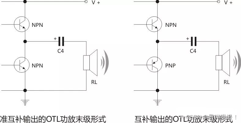
Yes, if they are connected in parallel. For a single NPN/PNP pair in a standard emitter-follower output stage, matching between the NPN and PNP is less critical because feedback linearizes the stage. However, if you have multiple NPN devices in parallel (or multiple PNP devices), matching them to each other is essential for preventing current hogging. Emitter resistors, proper bias compensation, and common heatsinking provide the main protection against thermal runaway.
What happens if I don't match the differential input pair?
You will likely see higher DC offset at the amplifier output — potentially hundreds of millivolts. This offset heats up the speaker voice coil even with no music playing. Unmatched pairs also produce higher even-order harmonic distortion, though this is usually masked by the negative feedback loop in typical designs [1].
Conclusion
Transistor matching is not a magic bullet for better sound, but it is a disciplined engineering practice that pays off in measurable ways: lower DC offset, more reliable parallel operation, and reduced distortion in specific circuit topologies. For the DIY builder working with discrete audio circuits, understanding which transistors to match — and how to do it — is an essential skill.
Start with transistors from the same hFE rank. Test at the currents your circuit actually uses. Control temperature carefully. Accept that ±10% is a practical, useful match. And if you need the ultimate in precision, consider a monolithic matched pair — two transistors on one die, sharing the same temperature and process, will outperform any hand-matched discretes.
Find More
- Building a Vintage Sound Power Amp with the 3AD56 Germanium Transistor
- 400W Power Stage 1 Pair K1058 / J162 FET Transistor Refer to Goldmund TELOS 300 Circuit Whole Aluminum Casing
- IWISTAO Hi-Fi Gold-sealed Matched Transistors Preamplifier Single-Ended Class A PCBA or Finished Unit
- IWISTAO HIFI Power Amplifier Finished Board 1 Pair 200W Golden Throttle A60 AC24VX2 ~ AC42VX2 DIY
References
- Self, Douglas. Audio Power Amplifier Design, 6th Edition. Focal Press, 2013. Chapter 7: "The Input Stage."
- Slone, G. Randy. High-Power Audio Amplifier Construction Manual. McGraw-Hill, 1999.
- Elliott, Rod. "Matching Power and Driver Transistors." Elliott Sound Products (ESP), 2025. https://sound-au.com/transistor-matching.htm
- Toshiba Semiconductor. "2SC2240 Datasheet: Silicon NPN Epitaxial Type (PCT Process)." https://handsontec.com/pdf_files/2SC2240.pdf
- ON Semiconductor. "MJL3281A / MJL1302A Datasheet: Complementary Power Transistors."
- Analog Devices. "MAT02: Low Noise, Matched Dual Monolithic NPN Transistor." https://www.analog.com/en/products/mat02.html
- THAT Corporation. "THAT 300 Series: Low-Noise Matched Transistor Arrays." http://www.thatcorp.com/300-series_Matched_Transistor_Arrays.shtml
- Diodes Incorporated. "Matched Pair Transistors." https://www.diodes.com/products/discrete-semiconductors/